top
본문
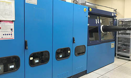
MOCVD
Maker
Application
- III-V Semiconductor Epitaxy for Optoelectronic Devices
- Laser Diodes
- Photodetectors
- Solar Cells
- High Speed Devices
- Source : TMGa, TMIn, TMAl, AsH3, PH3 * Very toxic gases
- Dopant : DEZn, Si2H4
- Growth Temperature : 550 ~ 680℃
- Growth Pressure : 100mbar
- Growth Rate : 0.5~4um/hr
Substrate
- InP wafer(2 inch, Piece * Piece : quarter of 2 inch)
- GaAs wafer(2 inch, Piece * Piece : quarter of 2 inch)
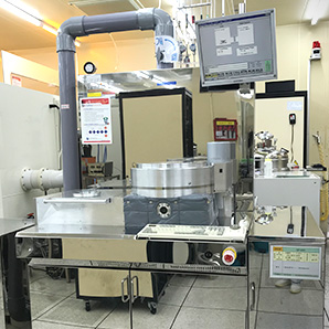
ICP
Maker
Application
- InP etch : HBr 15sccm, RF 100w, ICP 500w, 3mTorr
- GaAs etch : HBr 15sccm, N2 2sccm, RF 100w, ICP 600w, 3mTorr
- AlGaAs etch : Cl2 9sccm, Ar 2sccm, H2 19sccm, RF 100w, ICP 500w, 3mTorr
Substrate
- InP Wafer(3 inch, Piece)
- GaAs Wafer(3 inch, Piece)
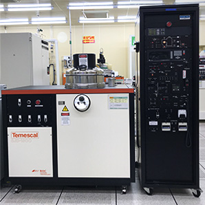
E-beam evaporator
Maker
Application
- Base Metal(Ti, Au), (Ti, Ni, Au)
- Heater Metal(Cr, Au), (Ti, Pt)
- T-Gate Metal(Ni, Au), FMT(Ti, Au), Backside metal(Ti, Au)
- P metal(Ti, Pt, Au) ,N metal(Cr, Au)
Substrate
- InP Wafer(2 inch~6 inch, Piece)
- GaAs Wafer(2 inch~6 inch, Piece)
- Si Wafer(2 inch~6 inch, Piece)
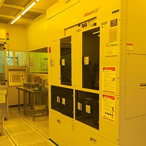
Lithography
Stepper
Application
- PROCESS/GANRF2017-2, PROGRAM/OPAD, EXP. TIME/400
- PROCESS/MZM17, PROGRAM/14, , EXP. TIME/800
- PROCESS/GANRF17E-MMIC, PROGRAM/DVIA, , EXP. TIME/340
- PROCESS/M-HEMT18-1, PROGRAM/RES, , EXP. TIME/40
Substrate
- GaAs wafer(4 inch, 3 inch, 2 inch)
- InP wafer(4 inch, 3 inch, 2 inch)
- GaN wafer(4 inch, 3 inch, 2 inch)