top
본문
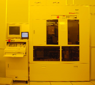
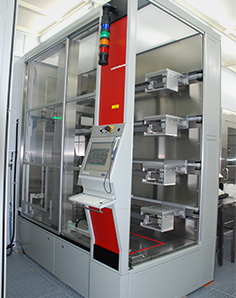
I-Line Stepper
Maker(model)
Application
- Resolution : 350nm
- Alignment Accuracy : 70nm or better(LSA, FIA)
- Exposure Area : 22mm square
- Reduction Ratio : 1:5
- Numerical Aperture : 0.63
- Reticle : 6 inch
Substrate
- Silicon Wafer, 6 inch
- Quartz Wafer, 6 inch(@ i11D)
- Glass Wafer, 6 inch(@ i11D)
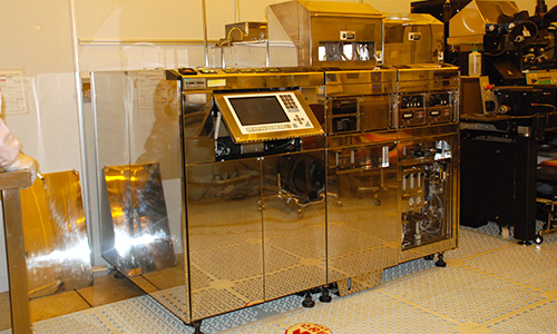
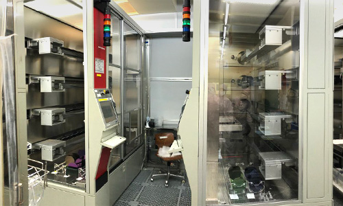
Track System
Maker(model)
- TEL(Mark-Vz), TSTI(Smart-cube)
Application
- Adhesion Treatment(HMDS) on Substrates
- Photo Resist Coating
- Development(TMAH) : Puddle&Spray
- Hot Plate Baking
Substrate
- Silicon Wafer, 6 inch
- Quartz Wafer, 6 inch(@TSTI)
- Glass Wafer, 6 inch(@TSTI)
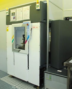
Dry Etcher
Maker
Application
- Oxide Etch
- Nitride Etch
- Poly-Si Etch
- Metal Etch
- PR Strip
Substrate
- Silicon Wafer(6 inch, Piece)
- Quartz Wafer(6 inch, Piece)
- Glass Wafer(6 inch, Piece)
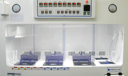
Wet Station
Maker
Application
- Standard Cleaning : H2SO4/H2O2 + 100:1 HF Cleaning
- SC1 Cleaning : NH4OH4/H2O2 + 100:1 HF Cleaning
- HF Cleaning : 50:1 BHF, 100:1 HF Cleaning
- DI Cleaning
- H3PO4 Etch : Nitride Strip @160℃
- Wet Etch : Oxide Etch, Metal Etch
- PR Strip : Acid PR Strip
Substrate
- Silicon Wafer(6 inch, Piece)
- Quartz Wafer(6 inch, Piece)
- Glass Wafer(6 inch, Piece)
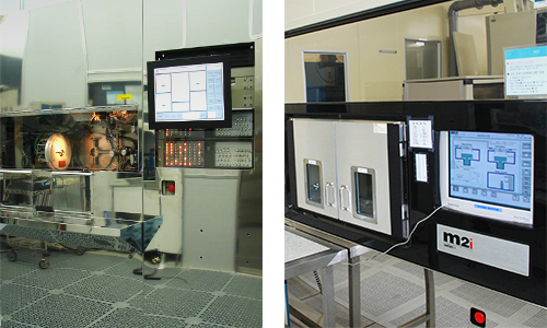
LPCVD
Maker
- centrotherm(E1550HT), 5Tube
Application
- TEOS Oxide : 710℃, 250mTorr, TEOS 40sccm
- Nitride, Low Stress Nitride
- 770℃, 250mTorr, NH3 300sccm, DCS 50sccm
- 825℃, NH3/DCS 30/150sccm ~ 50MPa Stress
- Poly Si/Amorphous Poly Si
- 625℃, 200mTorr, SiH4 72/68sccm
- 530℃, 200mTorr, SiH4 72/68sccm
- LTO : 425℃, 160mTorr, SiH4 160sccm, O2 160sccm
- HTO : 850℃, 350mTorr, DCS 40sccm, N2O 160sccm
- SiON : 850℃, 200mTorr, NH3 20sccm, DCS 20sccm, N2O 80sccm
Substrate
- Silicon Wafer(6 inch, Piece Thickness : 1mm 이하)
- Quartz Wafer(6 inch, Piece Thickness : 1mm 이하)
- Glass Wafer(6 inch, Piece Thickness : 1mm 이하)
PECVD
Maker
Application
- Oxide : 400℃, 3Torr, SiH4 60sccm, N2O 1200sccm
- Nitride : 400℃, 4.5Torr, SiH4/NH3/N2 185/75/1800sccm
- TEOS : 400℃, 5Torr, O2/He/TEOS 950/560/950sccm
- SACVD BPSG : 480℃, 200mTorr, O3 4000sccm, TEOS/TEB/TEPO 500/187/68mgm
- Oxynitride : 400℃, 4Torr, SiH4/N2O/N2 160/80/1000sccm
- Ge Oxide : 400℃, 3Torr, SiH4 80sccm, N2O 1200sccm, GeH4
Substrate
- Silicon Wafer(6 inch, Piece)
- Quartz Wafer(6 inch, Piece)
- Glass Wafer(6 inch, Piece)
Sputter
Maker
Application
- Al-1%Si : 200℃, 4.2KW
- TiW : 100℃, 3KW
- NiV, Cr, Mo : 100℃, 1.2KW, Variable Condition
- Ti, TiN : 400℃, 2.4KW(Ti), 7.2KW(TiN)
- AlN : 200℃, 1.9KW, N2/Ar 65/13sccm
- NbN : 상온, 2.4KW, N2/Ar 20/20sccm
- Pure Al, Al-1%Si : 200℃, 9.6KW
Substrate
- Silicon Wafer(6 inch, Piece)
- Quartz Wafer(6 inch, Piece)
- Glass Wafer(6 inch, Piece)
Furnace
Maker
Application
- Alloy : 400 ~ 460℃
- Wet/Dry Oxidation, Anneal, Drive-in
- 800 ~ 1250℃
- P-type Wafer Process
- Wet/Dry Oxidation, Anneal, Drive-in
- 800 ~ 1250℃
- N-type Wafer Process
- Dry Oxidation, Anneal : 800 ~ 1250℃
- POCl3 Doping : 800 ~ 900℃
Substrate
- Silicon Wafer(5 inch, 6 inch, Piece Thickness : 1mm 이하)
- Quartz Wafer(5 inch, 6 inch, Piece Thickness : 1mm 이하)
- Glass Wafer(5 inch, 6 inch, Piece Thickness : 1mm 이하)
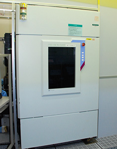
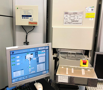
RTA
Maker
- Kornic System(Korona 600S)
Application
- RTA : Ar or N2 Ambient, 600 ~ 1100℃
Substrate
- Silicon Wafer(6 inch, Piece)
Ion Implant
Maker
Application
- Medium Current Ion Imp.
- BF2, B11, Ph Ion
- Max 180KeV
- Ion Dose : ~ 1E14
Substrate
- Silicon Wafer(6 inch, Piece)
Ion Implant
Maker
Application
- High Current Ion Imp.
- BF2, B11, Ph, As Ion
- Max 180KeV
- Ion Dose : ~ 1E16
- Max 18ea Wafer Loading
Substrate