

ICT TREND
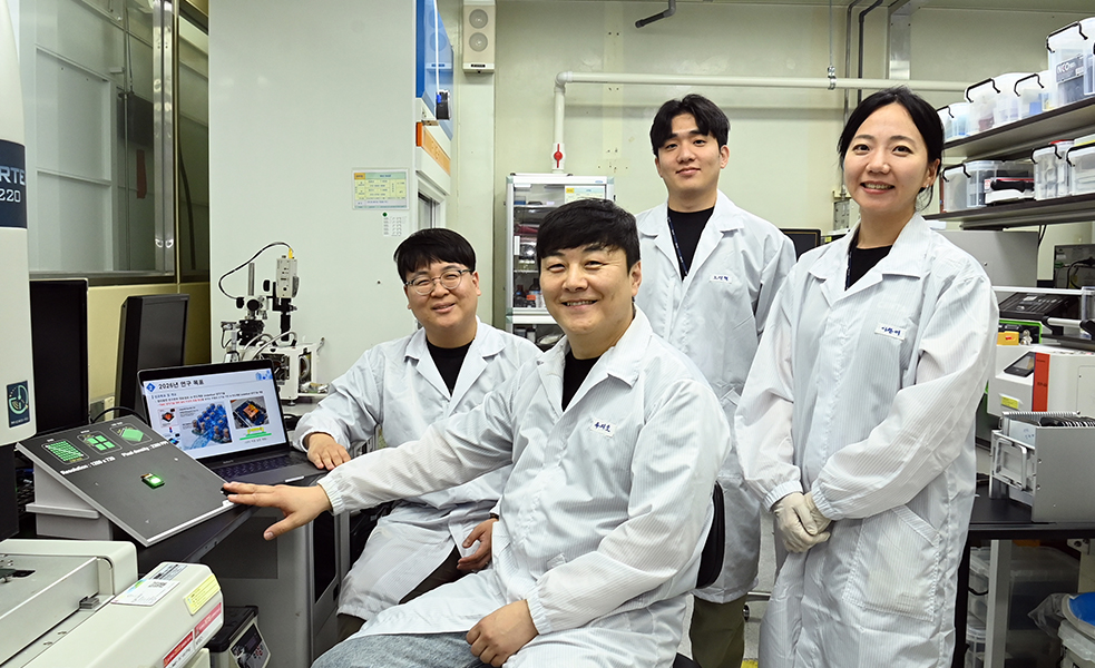
Korean researchers have developed core technology for ultrahigh-resolution displays for AI and XR. Using independently developed new materials and a laser process, the researchers realized ultrahigh-density bonding that is denser than HBM4 (High Bandwidth Memory 4)1)HBM4 (High Bandwidth Memory 4): A latest-generation, ultrahigh-performance DRAM that maximizes data processing speed by vertically stacking multiple DRAM chips., considered one of the most advanced semiconductor packaging technologies. The technology is expected to be widely used not only in next-generation XR devices but also in the AI semiconductor field.
ETRI announced that it has succeeded in developing ultrahigh-resolution LEDOS (Light Emitting Diode on Silicon)2)LEDOS (Light Emitting Diode on Silicon): A next-generation microdisplay technology made by precisely arranging ultra-small inorganic light-emitting diodes (LEDs) on a silicon wafer. It is a key component used in virtual reality (VR) and augmented reality (AR) devices that require ultrahigh resolution, ultra-small size and ultra-high brightness. display technology, which is drawing attention as a core display for the AI and XR era, as well as ultrahigh-precision laser bonding technology to implement it.
The research results were unveiled at SID Display Week 2026, the world’s largest display conference, and their technological excellence was recognized internationally when they won the People’s Choice Award in the micro-LED category.
The newly developed technology consists of 2500PPI-class ultra-highly integrated3)2500PPI-class ultra-high integration: Ultra-high resolution display technology in which more than 2,500 pixels are densely arranged within one inch. It is a core technology for realizing lifelike images in augmented reality (AR) and virtual reality (VR) devices, which enlarge screens directly in front of the eyes, beyond smartphone displays of about 400 to 500PPI. micro-LED display technology for AI-XR converged intelligent visual interfaces and an ultrahigh-precision laser bonding process that enables it. The researchers secured ultrahigh-density bonding technology capable of stably bonding about 920,000 bumps in a 10㎛(micrometer)-class pitch environment. This requires a much higher level of integration than the approximately 20㎛pitch and roughly 200,000 bumps of HBM4, which is currently attracting attention as a core AI semiconductor technology.
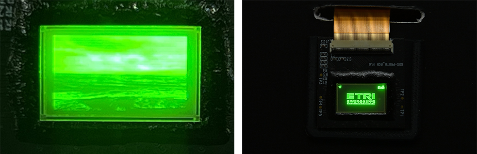 Actual photo of a SITRAB-based, ultra-high-density 2500 PPI Micro-LED display
HBM is a leading advanced semiconductor packaging technology used in AI accelerators, high-performance GPUs and other devices, and is regarded in the industry as a symbol of ultrafine, highly integrated interconnect technology. ETRI’s technology is significant in that it realized bonding conditions finer and more complex than those of HBM4 through a relatively economical process.
In conventional ultrafine bonding processes, major challenges have included substrate warpage caused by high-temperature processing, the generation of fine contaminants and bonding-position errors. In processes such as micro-LED assembly, where hundreds of thousands or more bumps must be bonded precisely at the same time, even small errors can sharply reduce yield.
To address this, the researchers applied a laser-based simultaneous transfer-and-bonding process using “SITRAB4)SITRAB (Simultaneous Transfer and Bonding): The world’s first simultaneous transfer and bonding technology developed by ETRI for micro-LED display manufacturing. The key to commercializing micro-LEDs is accurately transferring millions of ultra-small LEDs onto a substrate, and SITRAB is an innovative technology that integrates this ‘transfer’ process and the ‘bonding’ process of placing them on the substrate into a single step.”, a new material independently developed by ETRI.
SITRAB has a “fume-less” characteristic that suppresses the generation of fine contaminants in the form of fumes5)Fume: Extremely fine solid particles generated when vaporized solid or liquid materials rapidly cool and condense in the air. during the laser process, and it can be processed on a room-temperature stage, reducing substrate deformation and alignment errors caused by thermal expansion.
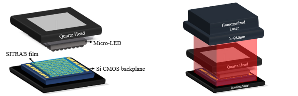 Schematic of the SITRAB material-based simultaneous transfer-and-bonding process technology
As a result, the researchers succeeded in stably bonding GaN-based6)GaN (Gallium Nitride)-Based: A technology that uses gallium nitride (GaN), a compound semiconductor material combining gallium (Ga) and nitrogen (N). Compared with silicon (Si), a conventional semiconductor material, it has lower power loss, faster switching speeds and less heat generation, making it a key technology for next-generation power semiconductors and high-frequency communication devices. micro-LED chips onto silicon CMOS circuits7)CMOS (Complementary Metal-Oxide Semiconductor): A core semiconductor technology and circuit design method most widely used to make integrated circuits (ICs) for modern electronic devices. It is an essential component in most digital devices, including smartphones, computer CPUs and memory., and completed the implementation of an ultra-high-resolution 2,500 PPI-class LEDOS display.
LEDOS is a next-generation microdisplay in which micro-LEDs are directly integrated on silicon CMOS circuits. Because XR devices such as AR glasses and VR headsets display images at close range in front of the eyes, they must integrate ultrahigh-resolution pixels into a very small area.
LEDOS can meet these needs by delivering ultrahigh resolution, ultrahigh brightness and low power consumption at the same time. In particular, it is regarded as a core display platform for the AI and XR era because it can provide clear images even in bright outdoor environments while consuming low power.
This achievement is also significant from the standpoint of commercialization. ETRI’s SITRAB materials technology has already been transferred to a Korean materials company, and the related process equipment has been applied to the mass-production line of a Korean outsourced semiconductor assembly and test (OSAT) company, where it is being validated in an actual manufacturing environment.
The achievement is considered meaningful because it has gone beyond a laboratory-stage research result and secured practical industrial applicability in connection with Korea’s materials, equipment and packaging industry ecosystem.
Jiho Joo, Director of ETRI’s Advanced Packaging Integration Research Section, said, “In the AI and XR era, it is very important to secure not only ultrahigh-resolution displays themselves but also ultrahigh-precision bonding technology that can actually manufacture them,” adding, “ETRI’s SITRAB-based LEDOS technology could be used beyond XR devices as a next-generation high-density heterogeneous integration platform.”
Kwang-Seong Choi, Assistant Vice President of ETRI’s Advanced Materials and Components Research Division, said, “This achievement demonstrates ultrahigh-density bonding at a level higher than HBM4 using only ETRI’s proprietary materials and process technologies, without relying on expensive overseas processes,” adding, “It will be applicable not only to AR glasses, VR headsets and microdisplays for defense and medical applications, but also to advanced semiconductor packaging.”
ETRI plans to continue developing technologies for RGB full-color implementation, ultralow-power operation and large-area scaling. It also plans to expand cooperation with Korean materials, equipment and packaging companies to strengthen the foundation for commercialization in next-generation displays and advanced packaging.
The research results were published May 11 in the leading international journal “Microsystems & Nanoengineering” (ranked in the top 0.6% by JCR category). This research was supported by the National Research Foundation of Korea’s Nano and Materials Technology Development Program, the Next-Generation Optical Packaging Technology Development Program, and ETRI’s internal R&D project.
Jiho Joo, Director
Advanced Packaging Integration Research Section
(+82-42-860-1832, jihojoo@etri.re.kr)