

SPECIAL
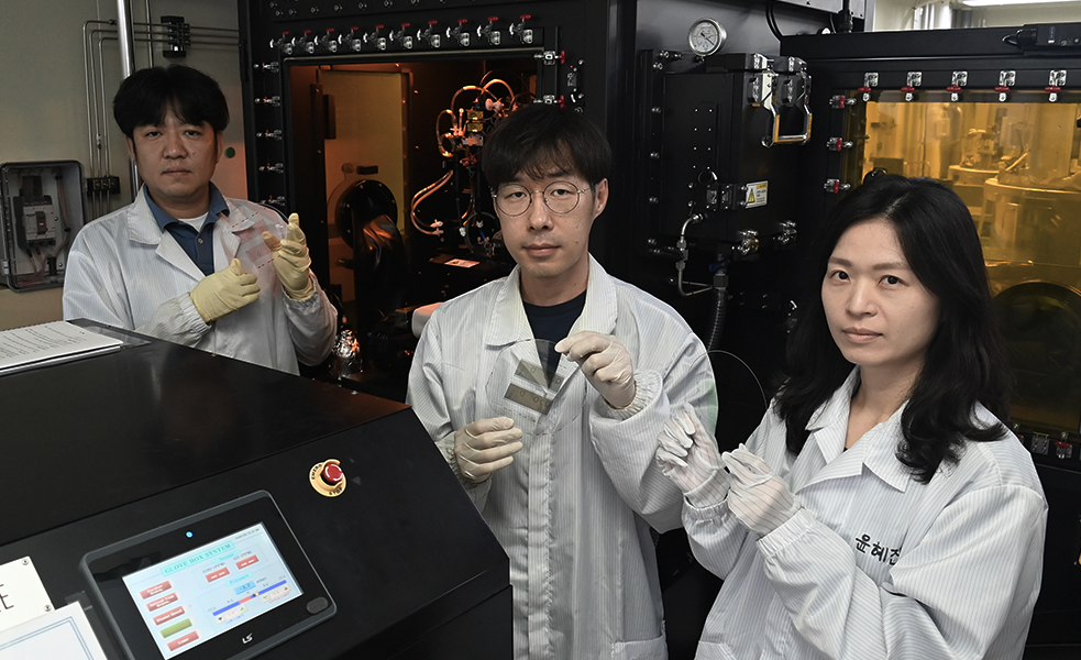
Korean researchers, working with display materials, parts, and equipment companies, have developed a process technology that can reduce the structural limitations of next-generation QD-OLED1)QD-OLED: A next-generation display technology that combines quantum dot (QD) technology and organic light-emitting diode (OLED) technology. Unlike conventional OLED methods, it provides overwhelming image quality by expressing pure and precise primary colors (red, green and blue). panels. The method stacks OLEDs and a QD color conversion layer2)QD color conversion layer: A functional layer that uses quantum dot (QD) materials to convert light emitted from a blue OLED into red and green light. A key pixel component that realizes vivid colors in QD-OLED. on a single substrate, and is seen as increasing the potential to realize thinner and more precise displays.
ETRI announced that, together with Gosan Tech Co., Ltd., Duksan Neolux Co., Ltd. and others, it has implemented “single-substrate stacked QD-OLED” panel technology using an industrial inkjet printing process3)Industrial inkjet printing process: A manufacturing process that forms patterns or thin films by precisely jetting ink-type materials through fine nozzles onto desired locations. In display manufacturing, this process is used to selectively form functional materials such as QD ink in pixel areas..
The achievement was published in 『Chemical Engineering Journal』, an international journal in the field of chemical engineering, earning recognition for both the technology’s originality and its potential industrial applications.
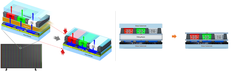 [Left] Schematic diagram comparing the display structures of commercial QD-OLED (left) and ETRI's single-substrate stacked QD-OLED (right)
 [Right] Schematic diagram comparing the display structures of commercial QD-OLED (left) and ETRI's single-substrate stacked QD-OLED (right)
QD-OLED is a display technology in which quantum dot (QD)4)Quantum dot (QD): A semiconductor nanoparticle material a few nanometers in size that emits or converts different colors of light depending on particle size. A key color conversion material that realizes high color purity and color reproducibility in displays. materials convert blue light emitted by OLEDs into red and green, producing vivid colors. Commercial QD-OLEDs currently generally use a structure in which a blue OLED light-emitting substrate and a QD color conversion substrate are manufactured separately and then bonded together. In this case, a filler layers5)Filler layer: A material layer formed to fill empty space between different substrates or layers. In QD-OLED, it fills the space between the blue OLED light-emitting substrate and the QD color conversion substrate and improves bonding stability. required between the two substrates, and added substrate alignment and bonding processes increase panel thickness and manufacturing complexity.
To reduce these limitations, the researchers applied a structure that forms a thin-film encapsulation (TFE)6)Thin-film encapsulation (TFE): A technology that seals OLED devices by stacking multiple layers of thin inorganic and organic films to protect them from moisture and oxygen. A key protective layer that ensures the lifespan and stability of OLEDs. layer over a blue OLED light source, then directly stacks a black pixel defining layer (Black PDL)7)Black pixel define layer (Black PDL): A black barrier structure that separates display pixel areas and prevents light from bleeding into neighboring pixels. It helps stably form QD color conversion layers in each pixel area and reduce color interference. and QD color conversion layer on top of it. Through this, they confirmed the feasibility of a process that can continuously fabricate the OLED light-emitting layer and QD color conversion layer on a single substrate without attaching a separate QD substrate. In particular, this achievement is the result of combining ETRI’s panel integration process capabilities with the materials and equipment technologies of Korean materials, parts and equipment companies.
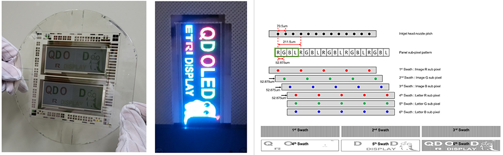 (Left) Photo of ETRI's single-substrate stacked QD-OLED display panel
 (right) Advancing the Multi-Pass Swath Printing Process: Precision Placement of QD Ink Within 184,800 Subpixels
The core of this technology lies in combining industrial inkjet printing equipment, low-temperature Black PDL materials and processes at or below 100℃, and QD ink materials technology into a single manufacturing flow. It is also significant in that the process was verified at the 6-inch-class panel level, rather than stopping at experiments at the unit-device level.
The work is particularly notable because it expanded the concept of COE (Color-filter-on-Encapsulation)8)Color-filter-on-Encapsulation (COE): A display stacking technology that forms color filters, black pixel define layers and other components on top of the OLED encapsulation layer. It is mainly used to reduce external light reflection and replace polarizers, thereby lowering panel thickness and power consumption. technology, which is used in premium smartphones and foldable OLEDs, to inkjet-based QD-OLED devices and implemented it at the panel level. Whereas conventional COE structures have mainly focused on reducing external light reflection, this research is differentiated by directly forming the QD color conversion layer inside the Black PDL walls, thereby integrating the color conversion function on a single substrate.
The QD color conversion layer is a core layer that converts blue OLED light into red and green. To achieve high color conversion efficiency, the QD color conversion layer must be formed with sufficient thickness, and to prevent light bleeding between neighboring pixels, the Black PDL partition walls that separate pixels must be made tall and precise.
However, conventional Black PDL materials had the problem that it was difficult to form tall partition walls and could degrade the performance of the lower OLED devices during high-temperature processes. In response, Duksan Neolux Co., Ltd. developed high-aspect-ratio Black PDL9)High-aspect-ratio Black PDL: A Black PDL structure precisely formed with a narrow width relative to its height. It has a barrier structure well suited to stably containing thick QD color conversion layers and reducing light bleeding between pixels. materials technology that can be formed stably even in low-temperature processes at or below 100℃, minimizing the impact on OLED devices.
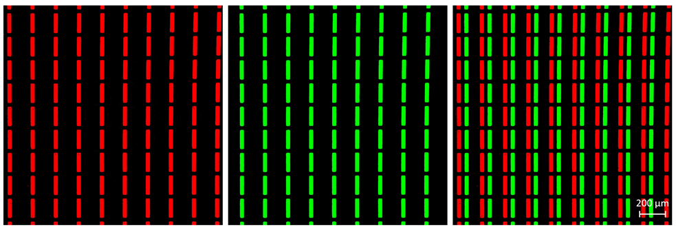 Photoluminescence characteristics of red/green QD pixels fabricated via industrial inkjet printing
Gosan Tech Co., Ltd. provided a head module and process control technology applicable to industrial inkjet printing processes. This established a process foundation for precisely dispensing QD ink into fine pixel areas and stably depositing it, even while using multi-nozzle-based inkjet heads.
ETRI integrated these materials, parts and equipment technologies to optimize the fabrication process for single-substrate stacked QD-OLED panels. The researchers implemented a QD-OLED panel with a total of 184,800 subpixels on a 6-inch substrate and achieved a pixel density of about 141ppi. This is similar to the pixel density required for 65-inch 8K TV-class displays.
Single-substrate stacked QD-OLED technology has the advantages of reducing panel thickness, simplifying the substrate bonding process and reducing alignment errors. In the future, its use is expected to expand not only to large premium displays but also to displays for mixed reality (MR)10)Mixed reality (MR): A technology that combines virtual information with real-world spaces so users can perceive and interact with both real and virtual content. It is a next-generation immersive display application field that combines the characteristics of virtual reality (VR) and augmented reality (AR). and extended reality (XR), which require thin form factors and high pixel integration density.
Principal Researcher Kwon Byoung-Hwa of ETRI’s Free-form Display Research Section said, “This research is an achievement that presents an industrial direction for next-generation QD-OLEDs by combining actual industrial inkjet printing technology, a QD color conversion layer and a Black PDL stacked pixel structure,” adding, “Having secured a full-cycle technology foundation spanning materials, processes and panel fabrication, we expect it to contribute to gaining an early lead in the future market for ultra-high-resolution mixed reality (MR) and extended reality (XR) displays.”
Meanwhile, this research was conducted with support from the Ministry of Trade, Industry and Energy and the Korea Evaluation Institute of Industrial Technology (KEIT) through the Industrial Technology Innovation Program “Development of Material, Component, and Equipment for Inkjet Printing in Flexible QD-OLED,” as well as ETRI’s core project “Research on Ultra-Realistic Spatial Device Technology.”
Kwon Byoung-Hwa, Principal Researcher
Free-form Display Research Section
(+82-42-860-1029, bhwak@etri.re.kr)