

SPECIAL
Korean researchers have secured flexible electronic skin technology that can be fabricated directly in the field. This achievement has further increased the feasibility of commercializing electronic skin for use in various fields, including robots and wearable devices.
Electronics and Telecommunications Research Institute (ETRI) announced that, in collaboration with the research team of Professor Ahn Jun Seong from the Department of Control and Instrumentation Engineering at Korea University's Sejong Campus, it has developed an in-situ process1)In-situ process: A method in which a process or experiment is conducted directly in the same environment or on site, without moving it to another location.-based electronic skin fabrication technology capable of producing large-area multimodal sensors2)Multimodal sensor: a sensor that simultaneously detects multiple sensory modalities. without a cleanroom, a dedicated semiconductor clean-processing facility.
Electronic skin is a thin, flexible sensor that detects pressure or contact like human skin and is a core technology that can be used to realize precise tactile sensing in intelligent robots.
Conventional flexible electronic sensors required semiconductor manufacturing processes such as photomask processing3)Mask process (Photomask Process): A process that creates a desired pattern by shining light through a template (mask)., vacuum deposition, and etching, necessitating costly cleanroom facilities and resulting in complex, expensive fabrication. In addition, because the process steps were divided into many stages, substrates had to be repeatedly moved, causing significant burdens in terms of process management and cost. As a result, there was a limitation in that process management became more complex when applying the technology to large areas or curved structures. In particular, attaching tactile sensors across broad surfaces, such as on humanoid robots with human-like forms, made it difficult to guarantee both process stability and reliability.
To address these limitations, the research team devised a maskless in-situ process4)Maskless in-situ process: A method of creating the desired pattern without using a template (mask). technology capable of fabricating sensors using only a UV laser5)UV laser: A laser that uses ultraviolet (UV) light and enables highly precise processing. and a 3D printer, eliminating the need for a separate mask process. This technology is designed to enable sensors to be fabricated on-site at the desired locations without the need for separate photomasks.
Using this approach, the team successfully demonstrated a large-area capacitive flexible tactile sensor array based on a microporous dielectric with high reproducibility in a short timeframe, thereby dramatically simplifying process steps to improve fabrication efficiency. The team also significantly reduced reliance on costly cleanroom facilities while securing both scalability and productivity for application-specific fabrication.
This technology is garnering attention in that it reduces the burden of the fabrication process while creating a fabrication environment applicable to various interactive systems, including intelligent robot tactile systems, human-machine interfaces (HMI)6)Human-Machine Interface (HMI): A technology that enables interaction between humans and machines, whereby the machine recognizes and responds to human touch or movement. Electronic skin is one form of HMI technology., and wearable devices.
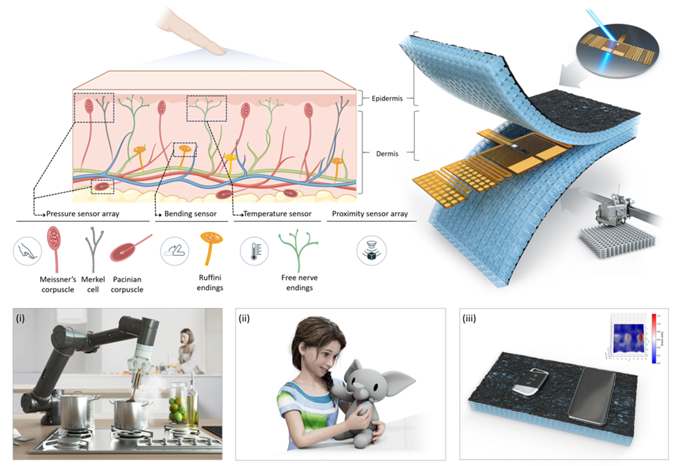 Large-area capacitive flexible sensor fabrication process and application examples
Sensors can be fabricated in a single continuous in-situ process without separation or transfer steps, and can be freely applied to objects with complex geometries including curved and contoured surfaces, offering a high degree of design flexibility. In addition, by supporting lower fabrication costs and rapid prototyping7)Rapid Prototyping: A technique for rapid prototype fabrication. at the same time, it can respond quickly to various application environments such as robotics, IoT devices, and healthcare.
ETRI demonstrated the technology's applicability in real-world robotic and human-machine interface environments by achieving implementation beyond the sensor device to the full system level. This achievement is regarded as having laid the groundwork for the practical application of next-generation intelligent robotic tactile systems and interactive electronic skin technology.
This research achievement was published in npj Flexible Electronics (IF 15.5), a leading international journal in the field of flexible electronic devices, earning recognition for its technical excellence.
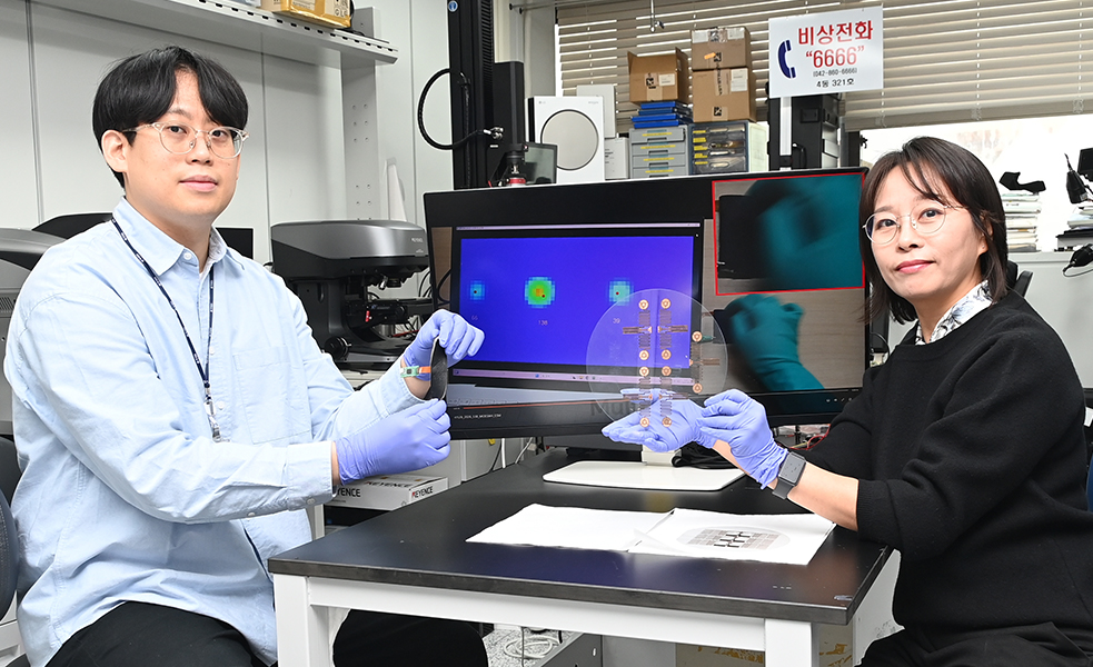
ETRI Principal Researcher Hye Jin Kim said, “This in-situ-process-based electronic skin technology is a key technology that significantly lowers the entry barriers to large-area flexible sensor fabrication while also taking the feasibility of implementing human-robot interaction technologies to the next level. The technology is expected to find applications with intelligent robots, wearable devices, and interactive systems more broadly.”
This research was conducted with support from the Ministry of Trade, Industry and Energy and the Korea Planning & Evaluation Institute of Industrial Technology (KEIT) through the K-Sensor Technology Development Project, as well as ETRI's core research program and Korea University’s support.
Hye Jin Kim, Principal Researcher
Intelligent Components and Sensors Research Section
(+82-42-860-6152, nolawara@etri.re.kr)