VOL. 65 june 2021
ETRI Solves
the Challenge in the Next Generation
Display Micro LED
- Transfer-Bonding processes combined into one process for the first time in the world...
Succeeded in developing the leading innovative technology
- Equipment investment & process time greatly reduced to 1/10, material & repair costs reduced to 1/100
-Materials developed in response to the materials, parts & equipment industry for application to TV & watch
The domestic research team developed the world’s first next-generation display technology that can simplify the process and reduce the incidental expenses considerably. The new materials required for the new process were also developed for the first time in the world and is expected to support the Korean industry considerably in continuing its leadership in the next-generation display market.
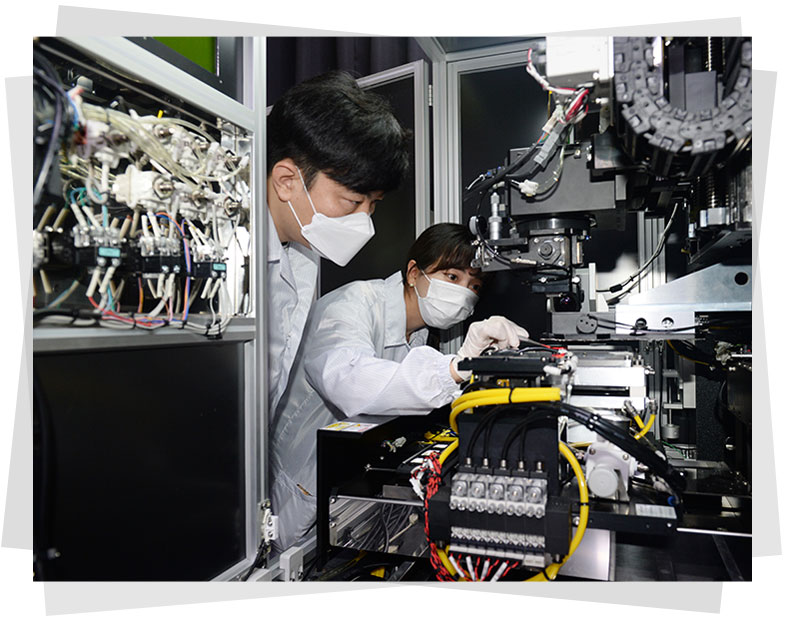
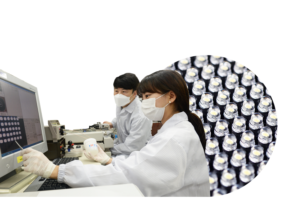
The Electronics and Telecommunications Research Institute (ETRI) announced that the new materials appropriate for the new technique were developed to solve the challenges in the micro LED1) display technique.
Micro LED display is a next-generation self-emitting display using micro LED2) as pixel light source. The research team fabricated 12 micro LEDs in 1㎟, and more vivid color can be realized compared to the LCD3) or OLED4)display. It also has such high luminous efficiency that it can be utilized in various fields such as TV and Smart watch, etc.
1) Measuring 1/10 of the mini-LED, the display uses micro-LED measuring about 10~100㎛
2) Light Emitting Diode (LED). Semiconductor device emitting light when applied with current in the forward direction
3) Liquid Crystal Display. The phenomenon of filtering the light when voltage is applied in the LCD, which has both properties of solid and liquid, is used.
4) Organic Light-Emitting Diode. The organic compound film emitting light by reacting to voltage is used.
Especially, micro LED display controls the RGB elements separately for the precise expression of screen brightness and color, and inorganic semiconductor can be used for a long period without worrying about the burn-in phenomenon of having quality deterioration
To develop the product, micro LED produced through the semiconductor process must be transferred to the display panel. For 8K TV, about 100 million micro LEDs are required, and the size is also very small that a long time for transfer and bonding is required. The materials required for manufacturing the display are also dependent on import, so the price is very high5).
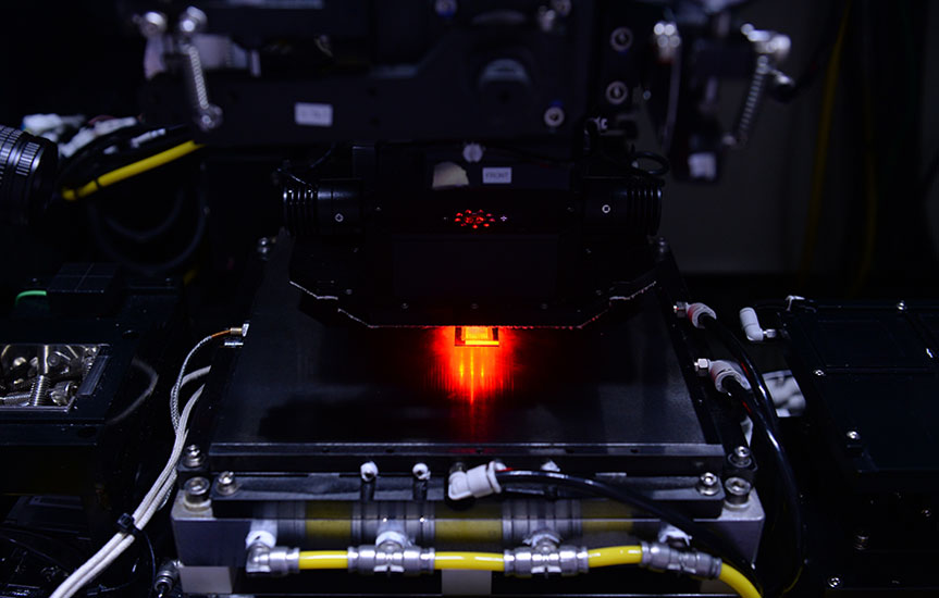
All existing methods were based on the sequential processes: the “transfer process” and then “bonding process.” The research team of ETRI developed the new materials, SITRAB6) adhesives, for use in combining the transfer and bonding processes into one process.
The research team applied homogenized laser to the SITRAB film attached to the micro LED for a few seconds to develop the core process of simultaneous transfer and bonding7) to overcome the challenge.
The key to this developed process is applying the homogenized laser to a large area but heating up only the part for attachment to mount the micro LED on a display panel substrate; this technique enabled preventing the inconvenience of performing the transfer and bonding processes separately. The new materials appropriate for the relevant technique was also developed independently to provide the opportunity to utilize the material not only for the micro LED but also on next-generation display technology such as mini-LED, etc.
By applying the technology developed by ETRI, the high investment costs that used to be required for the transfer and bonding equipment can be reduced, and the process can be simplified to increase the manufacturability. In addition, the newly developed materials can be attached with additional micro LEDs even when applied with laser several times for enhanced convenience of repairing the defective pixels8). Therefore, the limitation of the existing process, i.e., not being able to perform repair, can be solved.
5) 110-inch TV newly launched in March by domestic electronics company: About KRW 170 million
6) SITRAB (Simultaneous Transfer and Bonding)
7) LAB (Laser-Assisted Bonding) Process: Bonding process of applying homogenized laser to the semiconductor chip or package for bonding
8) Repair or Rework of defective pixel after transfer and bonding (Detaching the existing LED to attach the new LED)
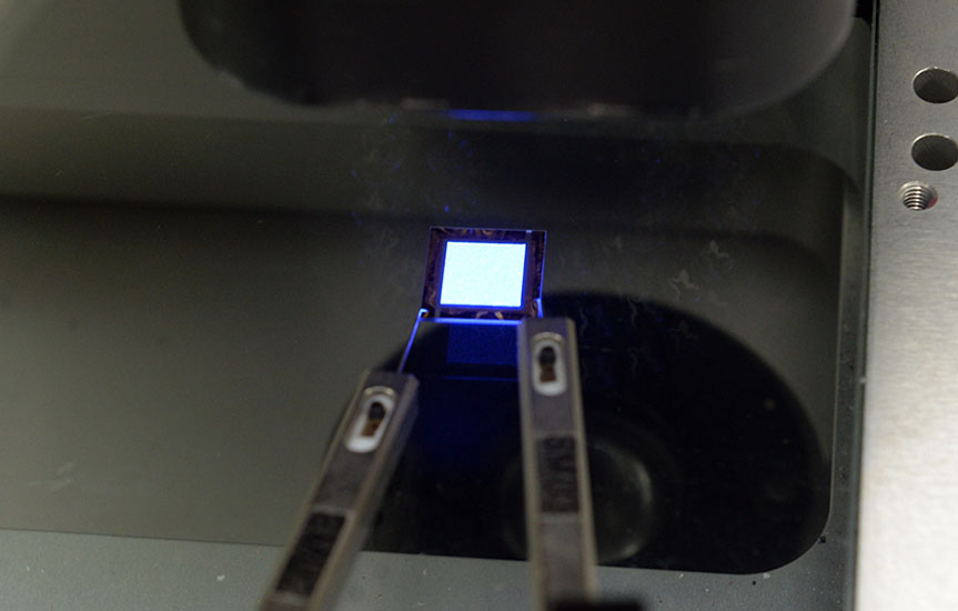
The micro LED, first presented by the research team was developed with blue color among the RGB, and the prototype with 1,225 micro LEDs in 100㎟ was demonstrated.
Especially, the transfer and bonding material that was mostly imported from Japan could be secured to create a new market through the new material development without the need for local manufacturing. The developed technology can also be utilized with domestically developed equipment instead of the expensive foreign equipment, making it favorable for commercialization.
By applying this ETRI-developed technology to the actual industrial field, the equipment investment cost and process time can be reduced to 1/10 compared to the existing technique, and the material and repair costs and time can also be decreased to 1/100 or less.
The research team attributed this result to efforts for the development of the relevant equipment and process based on know-how researched on the differentiated new material technology for 16 years by ETRI. ETRI expects the relevant products such as smart watch and TV, etc. to be commercialized within 2 years by transferring the technology to domestic display companies, etc.

“In the R&D field where global display companies are competing, ETRI became the first institution to overcome the limitations of the existing display. ETRI will continue the efforts to enable Korea to become the leader in the next-generation display and to maintain its status as the country with leading technology,” said Dr. Choi, Kwang-Seong, the multi-functional material team leader for micro LED in ETRI and Ministry of Science & Technology.
his research was conducted with the support of the 『Material Innovation Leading Project』 by the Ministry of Science and Technology, with the Korea Institute of Science & Technology, Korea Institute of Ceramic Engineering & Technology, and Korea Institute of Industrial Technology participating as joint research institutes.
The research team announced the technology through the Latest-News Paper9) in the 2021 SID Display Week, the world’s largest display symposium; thus enabling the excellence of the technology to be acknowledged.
According to the 2020 report by market survey company Omdia, the micro LED market is forecast to record an annual average growth rate of 65% until 2027 to have the relevant market scale reach USD 71 billion. The supply of LED Smart Watch is also expected to exceed 10 million, with micro LED TV exceeding 3.3 million as well.
Through this simultaneous transfer-bonding technology and process technology of applying new material to the laser, ETRI applied and registered 32 patents and presented 5 relevant theses.
9) Thesis Title: Simultaneous Transfer and Bonding (SITRAB) Process for Mini-LED Display